Introduction
As electronic systems continue to advance, operating frequencies increase, and packaging densities rise, the management of signal and power integrity (SI/PI) in printed circuit board (PCB) designs has become a foundational challenge. High-speed interconnects, crucial for modern computing, communication, and automotive systems, are highly susceptible to performance degradation from signal reflections, crosstalk, electromagnetic interference (EMI), and voltage fluctuations. Unmitigated SI/PI issues can lead to intermittent failures, reduced product reliability, and significant delays in design cycles due to costly re-spins.
Addressing these complexities necessitates a rigorous, managed engineering workflow that integrates advanced analysis techniques from the earliest stages of design. The objective is to proactively identify and mitigate integrity risks, ensuring robust product performance and accelerating time to market.
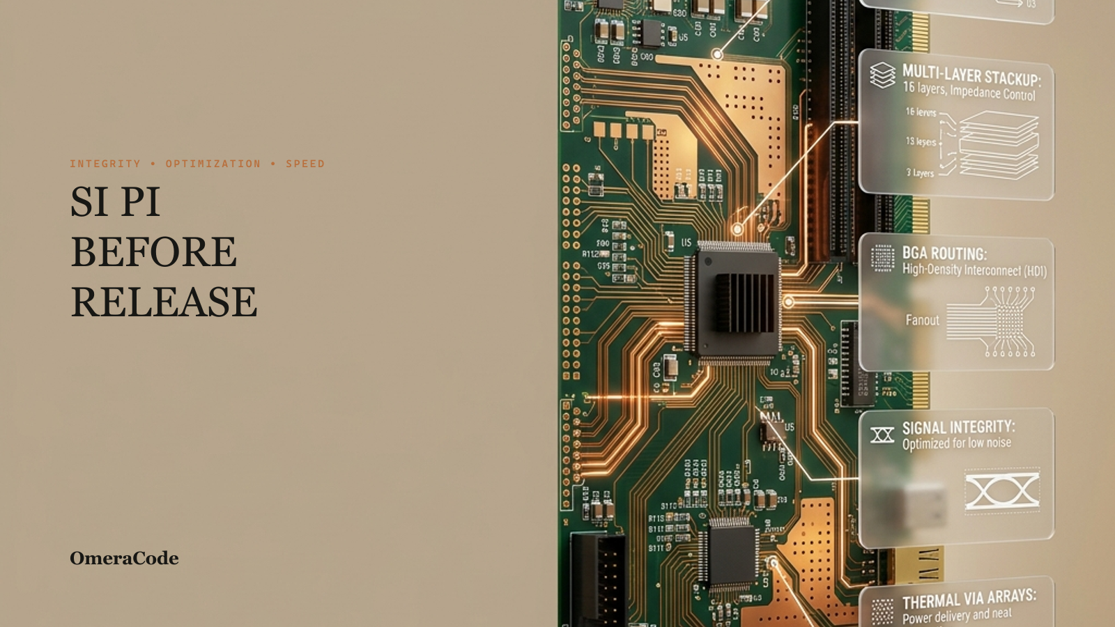
The Evolving Challenge of High-Speed Interconnects
Modern high-speed PCBs frequently incorporate gigabit-per-second data rates, demanding precise control over impedance, propagation delay, and loss. Power delivery networks (PDNs) must supply stable voltage rails with minimal noise across a wide frequency spectrum, often requiring multi-layered boards with complex vias and planes.
Traditional lumped-element models and 2D approximations often prove insufficient for accurately characterizing these behaviors. Key challenges include:
- Complex Geometries: Interconnects involving non-uniform traces, vias, and adjacent structures create intricate electromagnetic interactions.
- Multi-Physics Interactions: The interplay between electrical, thermal, and mechanical stresses further complicates performance prediction.
- Frequency-Dependent Behavior: Material properties and transmission line characteristics vary significantly with increasing frequency.
- Power-Signal Coupling: Noise from power delivery networks can couple into sensitive signal paths, and vice versa.
These factors necessitate the application of advanced 3D electromagnetic field solvers capable of full-wave analysis to accurately model the distributed effects that dominate at high frequencies. Such solvers provide a detailed understanding of electric and magnetic fields, current distributions, and resulting S-parameters, crucial for predicting true system behavior.
Integrated Workflow for SI/PI Assurance
OmeraCode emphasizes a comprehensive, managed PCB workflow that systematically addresses SI/PI challenges throughout the design lifecycle. This approach integrates advanced analysis into key design phases, ensuring traceability and verification.
1. Requirements Definition and Governance
The foundation of any successful design is a clear set of requirements. For high-speed PCBs, this includes:
- Performance Specifications: Data rates, timing margins, impedance targets, voltage tolerances.
- Protocol Compliance: Adherence to industry standards (e.g., PCIe, DDR, Ethernet) with their specific SI/PI guidelines.
- Environmental Constraints: Operating temperature, humidity, and EMI/EMC limits.
- Manufacturing Constraints: Material choices, stack-up definitions, layer count.
These requirements serve as the bedrock for all subsequent design and analysis activities, providing measurable criteria for validation. Robust requirements governance ensures that all design decisions are traceable back to these specifications.
- The OmeraCode Solution: OmeraCode allows engineering teams to codify electrical requirements, stackup constraints, and target impedances directly into the design schema, establishing automated compliance checks that flag violations early in the design cycle.
2. Early-Stage Design and Pre-Layout Analysis
Proactive identification of SI/PI risks begins before detailed layout.
- Architecture Analysis: Selecting appropriate components, connectors, and stack-ups.
- Conceptual Modeling: Using simplified 2D or basic 3D models to explore “what-if” scenarios for critical interfaces. This includes preliminary investigations into trace routing strategies, via structures, and power plane distributions.
- Constraint Generation: Translating requirements into design rules and constraints for the layout tool, guiding initial placement and routing.
This iterative analysis helps establish fundamental design parameters that reduce the likelihood of discovering major issues later in the design cycle.
- The OmeraCode Solution: The platform supports early-stage stackup planning and via structure pre-layout analysis, generating routing constraint sets that automatically guide subsequent layout tasks before physical routing begins.
3. Advanced Electromagnetic Simulation
Once a preliminary layout or critical interconnect segments are defined, advanced simulation tools become indispensable. Full-wave 3D electromagnetic field solvers are employed to analyze complex structures where simplifying assumptions are no longer valid.
- Signal Path Analysis: Characterization of impedance discontinuities, reflections, crosstalk between adjacent traces, and insertion/return loss for critical high-speed signals.
- Power Delivery Network (PDN) Analysis: Assessment of impedance profiles, voltage droop, ground bounce, and decoupling capacitor effectiveness across the board. This includes simulating the interaction between power planes, vias, and components.
- Frequency-Domain and Time-Domain Analysis: Generating S-parameters to understand frequency response and converting these to time-domain waveforms to observe actual signal transitions, eye diagrams, and transient noise.
Computational frameworks can be integrated with these solvers to optimize simulation parameters, manage large models efficiently, and accelerate analysis through distributed computing or intelligent model simplification techniques where appropriate.
- The OmeraCode Solution: OmeraCode integrates with full-wave 3D solvers (like Clarity/ACE) to automate parameters extraction, returning return path impedance profiles and S-parameters directly to the human review interface.
4. Design Rule Checks (DRC) and Design for Manufacturability (DFM)
The insights gained from SI/PI simulations are integrated with traditional DRC and DFM processes.
-
Custom SI/PI Rules: Development of specialized design rules based on simulation findings, such as minimum trace spacing for crosstalk mitigation or via stitching requirements for return path continuity.
-
Automated Verification: Tools can perform automated checks against these custom rules, ensuring compliance across the entire layout.
-
Manufacturing Feasibility: Aligning SI/PI optimized designs with manufacturing capabilities to avoid issues like excessive trace width variations or unfeasible drill aspect ratios that could negatively impact performance or yield.
-
The OmeraCode Solution: Custom spacing and clearance rules are continuously verified against the physical board geometry during routing. If any constraint is violated, the system blocks the release pipeline at the DFM check step.
5. Automated Verification and Evidence Generation
A critical aspect of a managed workflow is the generation of a comprehensive “evidence pack.” This pack serves as documentation for design decisions and verification outcomes.
- Simulation Reports: Detailed outputs from all SI/PI analyses, including eye diagrams, S-parameter plots, voltage ripple data, and impedance profiles.
- Compliance Matrix: A matrix mapping each design requirement to its corresponding verification method and results, ensuring all specifications have been validated.
- Design Rule Check Reports: Documentation of all DRC and DFM checks performed.
Automated frameworks can consolidate these results, providing a clear, auditable record that substantiates the design’s integrity. Such automation enhances consistency and reduces manual effort in documentation.
- The OmeraCode Solution: OmeraCode programmatically compiles all design checks, DRC violations history, and simulation outputs into a signed, immutable Evidence Pack (.epk), providing a single source of truth for peer and release reviews.
Ensuring Manufacturing Readiness and Human Release Review
The culmination of this structured workflow is manufacturing readiness. Before releasing a design for fabrication, a final, thorough review by experienced engineers is paramount.
- Consolidated Review: A multidisciplinary team reviews the entire evidence pack, including all SI/PI analysis results, DRC/DFM reports, and compliance matrices.
- Risk Assessment: Any remaining identified risks are evaluated, and mitigation strategies are confirmed or accepted.
- Human Judgment: While advanced tools provide critical data, the ultimate decision to release a design rests with human engineers. Their expertise is essential for interpreting complex simulation results, considering potential real-world variations, and making informed trade-offs.
This final human release review ensures that the design is not only technically sound according to simulations but also robust and manufacturable within practical limits.
Conclusion
The escalating demands of high-speed electronics necessitate a sophisticated and integrated approach to SI/PI analysis. By embedding advanced electromagnetic simulation into a managed PCB workflow, from requirements definition through to final manufacturing readiness, engineers can proactively address complex integrity challenges. This systematic methodology, supported by robust verification and a critical human release review, leads to highly reliable, performant, and cost-effective electronic products.
Further Reading
For additional insights into advanced electromagnetic simulation techniques and their application in streamlining SI/PI analysis, consider the following:
- Cadence. “Streamlining SI/PI Analysis with Clarity 3D Solver’s New ACE Technology.” Cadence Community Blog, 2 Apr 2026. https://community.cadence.com/cadence_blogs_8/b/pcb/posts/streamlining-si-pi-analysis-with-clarity-s-new-ace-technology